

Product
Product Details
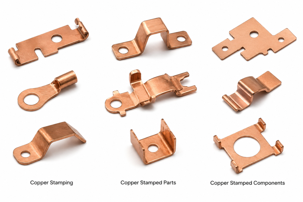
Copper Stamping and Copper Stamped Parts
Copper Stamping and Copper Stamped Parts
Pricing: US$ 16.80 / Kilogram (FOB India | MOQ: 50 Kg | Custom grades on request)
Electrical Accessories India manufactures and exports precision copper stamping and copper stamped parts produced from high-conductivity electrolytic tough pitch (ETP) copper, oxygen-free high conductivity (OFHC) copper, and phosphorus-deoxidized (DHP) copper sheet and strip stock. These copper pressed components are manufactured on mechanical and hydraulic presses using progressive dies, compound dies, and transfer dies, conforming to customer-supplied 2D drawings or 3D CAD models. Copper stampings serve electrical OEMs, switchgear manufacturers, transformer manufacturers, EPC contractors, power utilities, and electronics subassembly producers across North America, Europe, the Middle East, and Asia-Pacific.
Product Overview – Copper Stamping and Copper Stamped Parts
Copper stampings—also referenced in procurement specifications as copper pressed parts, copper sheet metal parts, copper die-cut parts, copper blanked components, copper formed parts, copper drawn components, and copper punched parts—represent a versatile category of high-conductivity copper components produced by controlled deformation of copper strip or sheet stock under press tooling. Unlike machined parts, stampings offer high production rates, minimal material waste through progressive strip layouts, and consistent dimensional repeatability across large production runs, making them the preferred manufacturing route for flat, semi-flat, and moderately formed copper electrical components.
Electrical Contact Stampings and Busbar Blanks
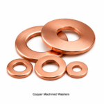
Copper contact blanks, busbar blanks, busbar end caps, flexible busbar connectors, contact bridges, shorting links, switchgear contact fingers, overload relay contacts, contactor contact tips, relay armature stampings, terminal lugs, connecting strips, and current-carrying shims are among the most commonly produced copper stamped parts for the switchgear and control gear industry. These parts are produced from C11000 ETP copper strip in thicknesses from 0.3 mm to 6 mm with conductivity exceeding 98% IACS.
Earthing and Grounding Stampings
Earth tags, earth clamp bodies, grounding strips, bonding straps, earthing washers, equipotential bonding plates, terminal bonding lugs, cable tray bonding clips, cable screen bonding tags, and grounding splice plates are produced as copper stampings for use in building earthing systems, substation earthing grids, surge protection installations, railway traction earthing, and ATEX/IECEx-rated hazardous area electrical installations. The excellent formability of ETP copper allows complex profiles to be produced in single progressive die strokes.
Transformer and Switchgear Stampings
Transformer winding end turn clamps, HV/LV terminal pads, transformer tie rods, coil support brackets, bus-duct spacers, bus-duct end closures, current transformer (CT) primary bar stampings, surge arrester terminal pads, GIS (Gas-Insulated Switchgear) contact blanks, vacuum interrupter contact discs, ring main unit (RMU) contact fingers, and cable box connecting plates are produced as precision copper stampings meeting dimensional tolerances of ±0.05 mm for critical mating surfaces.
Electronic and Instrumentation Stampings
PCB bus bars, shielding frames, EMI/RFI shielding cans, SMT (surface-mount) copper heat spreaders, current sense shunts, battery terminal stampings, fuse clips, fuse end caps, circuit breaker bimetal supports, connector lead frames, relay base stampings, thermocouple compensating strip blanks, and copper spring contacts are produced from phosphorus-deoxidized C12200 or tellurium copper C14500 strip for applications requiring precise spring-back control, solder wettability, or free-machining secondary operations.
Custom Deep-Drawn and Formed Copper Stampings
Deep-drawn copper cups, copper shells, copper caps, copper contact rivet heads, drawn contact discs, dome-shaped stampings, hemispherical contact caps, shallow-drawn cable gland bodies, copper ferrule blanks, cup-and-flange terminals, electrical socket contacts, drawn bushing blanks, and axially drawn cylindrical contacts are produced on hydraulic presses with progressive draw tooling. Draw ratios up to 2.5:1 are achievable in ETP copper without intermediate annealing for parts up to 50 mm diameter.
Progressive Strip Stampings and Multi-Station Parts
Multi-hole busbar strips, progressive terminal strip stampings, ladder-type conductor strips, louvered ventilation stampings, perforated copper filter mesh, EMI honeycomb vent stampings, multiple-contact spring strips, connector carrier strips, auto-insertion terminal strips, and multi-up contact lead frames are produced on progressive dies running at 100–400 strokes per minute with coil-fed strip automation, offering the highest economy of scale for volumes exceeding 50,000 pieces per order.
Special Alloy and Plated Copper Stampings
Beryllium copper (C17200) spring stampings, phosphor bronze (C51000) contact stampings, tin-bronze contact blanks, silver-bearing copper (C11600) stampings, and tellurium copper (C14500) precision stampings are available for specialized applications. Post-stamping surface treatments include tin plating (ASTM B545), nickel plating (ASTM B689), silver plating (ASTM B700), gold flash, palladium plating, and chemical passivation for tarnish resistance in tropical and offshore environments.
Key Features of Copper Stampings
- Material grades: C10100, C11000, C12200, C14500, and copper alloys per customer specification
- Thickness range: 0.2 mm to 6 mm (sheet and strip fed)
- Part size range: 5 mm to 500 mm maximum dimension
- Dimensional tolerance: ±0.05 mm standard; ±0.02 mm precision grade
- Conductivity: 98–101% IACS (C10100/C11000 grades)
- Progressive die, compound die, and transfer press operations
- 100% dimensional check per AQL 1.0; conductivity testing per batch
- RoHS 2 and REACH compliant alloys and surface treatments
High Electrical and Thermal Conductivity
ETP copper (C11000) delivers ≥ 98% IACS electrical conductivity and thermal conductivity of 391 W/m·K — values that cannot be matched by aluminium, brass, or stainless steel stampings. These properties make copper stampings indispensable for current-carrying components in power distribution panels, switchgear, transformer terminals, and earthing systems. For applications requiring the highest purity, OFHC C10100 copper (≥ 99.99% Cu, ≤ 0.0005% O₂) is used, achieving ≥ 100% IACS conductivity, meeting IEC 60317 requirements for winding conductors and bus connections.
Precision Dimensional Accuracy
Progressive die tooling manufactured on CNC wire EDM machines to DIN ISO 2768 tolerances ensures part-to-part dimensional repeatability within ±0.05 mm for general stampings and ±0.02 mm for precision contact stampings. Critical hole positions, punched slots, and formed bends are maintained through die-set guidance, stripper plates, and pilot pin alignment. First-article inspection (FAI) per AS9102 / PPAP Level 3 is available for OEM qualification programs. All tooling is maintained in-house for rapid changeover and short lead times on repeat orders.
Versatile Forming Capability
Blanking, piercing, notching, lancing, embossing, coining, bending, forming, deep drawing, thread forming, and staking operations are performed on the same progressive die in a single press stroke sequence, eliminating secondary operations and reducing piece-part cost. Multi-slide forming, roll forming, and rotary notching are available for special profiles. Copper’s superior formability — elongation 40–45% for annealed ETP — ensures complex bent and drawn profiles can be produced without cracking, tearing, or spring-back issues that would affect harder materials.
Material Traceability and Certification
All copper coil and strip stock is sourced from LMBA-registered smelters with EN 10204 Type 3.1 mill certificates confirming chemical composition, tensile strength, hardness, and conductivity. Heat number traceability is maintained through production lot records. Incoming material is tested by ICP spectrometry for composition verification and eddy-current instrument for conductivity confirmation before release to production. Third-party witnessed inspection by SGS, Bureau Veritas, or TÜV is available for large OEM orders.
Surface Treatments and Secondary Operations
Post-stamping operations include deburring (vibratory finishing, barrel tumbling), electroplating (tin, nickel, silver, gold), chemical passivation, lacquering, annealing (bright annealing in H₂/N₂ atmosphere), and laser or ink marking. Assembled sub-components — including inserts, riveted contacts, and welded assemblies — are accepted as value-added services. Packaging options include bulk bags, compartmented trays, blister packs, or custom customer-specified packaging with ESD (electrostatic discharge) protection for sensitive contact parts.
Cost Efficiency and Lead Time
Progressive die stamping from copper coil stock offers the lowest per-piece cost for medium to high-volume production (5,000 pieces and above). Strip utilisation efficiency of 75–90% is achieved through optimised blank layouts calculated by CNC nesting software. Standard tooling lead time is 3–5 weeks for new progressive dies; repeat production runs are fulfilled within 2–3 weeks. Low-volume prototype stampings from sheet blanks can be produced in 7–10 days for R&D and type-approval requirements. Kanban and blanket order supply programmes are available for OEM customers with stable monthly requirements.
Technical Specifications
| Parameter | Specification |
|---|---|
| Product | Copper Stamping / Copper Stamped Parts |
| Process | Progressive Die Stamping, Compound Die Stamping, Deep Drawing, Transfer Press |
| Material Grades | C10100, C11000, C12200, C14500 (see grade table) |
| Strip/Sheet Thickness | 0.2 mm to 6.0 mm |
| Part Size Range | 5 mm min. to 500 mm max. characteristic dimension |
| Dimensional Tolerance | ±0.05 mm standard; ±0.02 mm precision grade |
| Flatness | 0.1 mm per 100 mm (standard); 0.05 mm/100 mm precision |
| Hole Position Tolerance | ±0.05 mm (standard) per ISO 2768-m |
| Conductivity | 98–101% IACS (grade dependent) |
| Tensile Strength | 200–380 MPa (temper dependent) |
| Hardness | 40–110 HRF (annealed to half-hard) |
| Surface Finish | Bright / Tin-plated / Nickel-plated / Silver-plated / Passivated |
| Production Volume | Prototype (100 pcs) to mass production (10 million+/year) |
| Lead Time | Tooling: 3–5 weeks; Production: 2–3 weeks (repeat) |
Copper Raw Material Grades and International Equivalents
| UNS (USA) | EN (Europe) | BS (UK) | DIN (Germany) | IS (India) | JIS (Japan) | Description |
|---|---|---|---|---|---|---|
| C10100 | CW008A | C101 | E-Cu99.99 | — | C1011 | OFHC – Oxygen-Free High Conductivity |
| C11000 | CW004A | C101 | E-Cu58 (ETP) | ETP Copper | C1100 | Electrolytic Tough Pitch (ETP) |
| C12200 | CW024A | C106 | SF-Cu (DHP) | DHP Copper | C1220 | Phosphorus Deoxidized High Residual |
| C14500 | CW118C | C109 | CuTeP | — | C1450 | Tellurium Copper – Free Machining |
| C17200 | CW101C | CB101 | CuBe2 | — | C1720 | Beryllium Copper (spring/contact grade) |
Product Types and Variants
| Stamping Type | Description | Typical Application |
|---|---|---|
| Flat Blanks | Single-hit blanked profiles, all shapes | Busbar blanks, contact pads, terminal pads |
| Pierced/Punched Parts | Blanks with punched holes, slots, notches | Connector terminals, busbar with bolt holes, earthing tags |
| Bent / Formed Parts | Single or multi-bend formed stampings | Cable clamps, spring contacts, terminal lugs |
| Deep Drawn Parts | Cups, shells, caps, cylindrical forms | Contact rivet heads, socket contacts, drawn bushings |
| Progressive Strip Parts | High-volume strip-fed multi-station stampings | Lead frames, terminal strips, contact fingers |
| Embossed / Coined Parts | Precision thickness control, embossed profiles | Contact tips, shunt elements, current-sensing parts |
| Compound Die Parts | Blank + pierce in one stroke | Earthing washers, sealing washers, ring terminals |
Applications by Industry
| Industry | Copper Stamping Application |
|---|---|
| Power Transmission and Distribution | Busbar blanks, substation grounding pads, transformer terminal stampings, cable clamp bodies |
| Switchgear and Control Gear | Contact fingers, contact bridges, shorting links, relay armatures, earthing strips |
| Renewable Energy | Solar panel junction box busbars, inverter terminal pads, battery interconnect strips |
| Automotive and EV | Battery terminal stampings, BMS bus bars, motor winding end-turn clips |
| Electronics and PCB Assembly | EMI shields, heat spreaders, contact lead frames, SMT pads, PCB busbars |
| Railways and Metro | OHE bonding straps, pantograph contact inserts, traction return bonding plates |
| Telecommunications | BTS earthing straps, data centre PDU busbars, rack bonding strips |
| Industrial Manufacturing | Machine tool earthing, motor terminal connections, variable speed drive busbars |
Manufacturing Process
Copper stampings are produced through a controlled multi-step manufacturing process. Step 1 – Incoming Material Inspection: Copper coil or sheet is tested for chemical composition (ICP spectrometry), conductivity (eddy-current instrument), and mechanical properties (tensile/hardness) before acceptance. Step 2 – Blank Layout and Die Design: Optimal strip layouts are designed using CNC nesting software to maximise material utilisation. Dies are manufactured on CNC wire EDM and CNC milling machines with hardened D2 or M2 tool steel punches and dies. Step 3 – Pressing/Stamping: Production runs on mechanical presses (30–400 tons) or hydraulic presses (up to 1000 tons) for deep drawing. Progressive dies run at 60–400 strokes/minute with coil-fed strip. Step 4 – Deburring and Cleaning: Parts are deburred in vibratory finishers using porcelain or ceramic media, then ultrasonically cleaned and dried. Step 5 – Surface Treatment: Plating, passivation, or lacquering is applied per customer specification. Step 6 – Inspection: 100% visual inspection; dimensional sampling per AQL 1.0 using optical comparators and CMMs; conductivity testing on 10% of pieces. Step 7 – Packing and Dispatch: Parts are packed in moisture-barrier VCI polybags, compartmented trays, or bulk containers with EN 10204 material certificates.
Quality Standards and Certifications
| Standard / Certification | Scope |
|---|---|
| ISO 9001:2015 | Quality Management System |
| ASTM B152 / BS EN 13599 | Copper sheet and strip chemical composition and properties |
| EN 10204 Type 3.1 | Material test certificate with independent inspection |
| DIN ISO 2768 | General tolerances for stampings |
| RoHS 2 (2011/65/EU) | Restriction of hazardous substances in surface treatments |
| REACH (EC 1907/2006) | Chemical substance compliance |
| ASTM B117 | Salt spray / corrosion testing (plated parts) |
| IEC 60068-2-52 | Salt mist cyclic test for plated components |
Why Choose Electrical Accessories India for Copper Stampings?
Electrical Accessories India operates dedicated copper stamping press lines equipped with mechanical and hydraulic presses from 30 to 400 tons, progressive die sets manufactured in-house on CNC wire EDM, and in-house electroplating facilities. Our capabilities include: single-source supply for copper stampings, machined parts, fasteners, and connectors; EN 10204 3.1 material certificates with every shipment; NABL-traceable dimensional and conductivity testing; tooling manufactured and owned in-house for competitive repeat pricing; export packaging per ISPM-15; and competitive pricing at US$ 16.80/kg FOB India. We supply clients in India, USA, UK, Germany, UAE, Australia, Canada, Singapore, and South Africa.
Frequently Asked Questions (FAQ)
Q1. What is the minimum order quantity for copper stampings?
MOQ is 50 kg for standard blank and pierced stampings. For tooled progressive die stampings, MOQ is 100 kg per design. Prototype orders of 100–500 pieces are accepted for OEM qualification at nominal tooling charges. Sample runs are facilitated through laser-cut or wire-EDM-cut blanks before hard tooling is committed.
Q2. What copper grade is recommended for electrical contact stampings?
C11000 ETP copper is standard for busbar and earthing stampings. C12200 DHP copper is preferred for stampings that will be silver-brazed, soldered, or welded, due to its deoxidised nature preventing gas porosity. C14500 tellurium copper is used where secondary CNC drilling or threading operations follow stamping. C10100 OFHC is specified for vacuum interrupter contacts and ultra-low oxygen applications.
Q3. Can you supply stampings with pre-punched bolt holes to customer drawings?
Yes. Hole patterns conforming to DIN, BS, ANSI, or customer-specific pitch are punched in the same progressive die operation as blanking. Hole diameter tolerance is typically H11 (+0.1/0 mm) for M3–M20 clearance holes. Square, elongated, and keyhole slot forms are also available.
Q4. What plating thickness is standard for tin-plated copper stampings?
Matte tin plating per ASTM B545 at 3–5 μm is standard for contact stampings. Bright tin at 5–8 μm is available for enhanced solderability. Nickel undercoat (2 μm) followed by tin (3 μm) is specified for anti-diffusion applications in high-temperature environments above 150°C.
Q5. What is the lead time for tooling a new progressive die?
Standard progressive die tooling lead time is 3–5 weeks from approved drawing. Complex multi-station dies with deep draw stages may require 6–8 weeks. First article samples are supplied with each new tool for customer approval before production release. Tool cost is quoted separately and amortised into piece price for volume orders above 50,000 pieces.
Q6. Do you offer copper stamping assemblies with inserts or hardware?
Yes. Secondary operations including press-in inserts (PEM or equivalent), riveted studs, spot welding, resistance welding, ultrasonic welding, and adhesive bonding are performed in-house. Sub-assembled copper stamping kits — for example, busbar assemblies with hardware and insulation — are available as complete ready-to-install units.
Q7. Are EN 10204 3.1 material test certificates provided?
Yes. EN 10204 Type 3.1 certificates from the copper strip mill are provided with every shipment, including chemical composition, mechanical properties, hardness, and conductivity data. Third-party inspection by SGS, Bureau Veritas, or RINA is available at additional cost.
Q8. What is the maximum strip thickness you can stamp?
Standard press capacity handles copper strip up to 6 mm thick. For heavier gauges up to 12 mm, fine-blanking or milling/sawing followed by pressing is used. For very large blanks exceeding 500 mm, waterjet or laser cutting from copper sheet is offered as an alternative to progressive die stamping.
Q9. Can copper stampings be supplied in a specific temper or hardness?
Yes. Strip stock is sourced in annealed (O), quarter-hard (H01), half-hard (H02), and hard (H04) tempers per ASTM B152 designations. Post-stamping annealing (bright anneal at 400–600°C in protective atmosphere) can be applied to restore ductility after cold working, particularly for deep-drawn parts. Specific hardness targets (HRF, HRB, or Vickers HV) can be specified on the order.
Q10. What industries do you export copper stampings to?
We export to the electrical switchgear, power transformer, renewable energy (solar/wind), automotive (EV battery systems), electronics, railway traction, marine, oil & gas, and telecommunications industries. Current export markets include the USA, UK, Germany, France, UAE, Saudi Arabia, Australia, Singapore, South Africa, and Canada. FOB India pricing with sea or air freight options is available.
Equivalent Terms in Other Languages
| Language | Equivalent Terms (3–4 terms) |
|---|---|
| Spanish | Estampaciones de cobre, Piezas estampadas de cobre, Partes troqueladas de cobre |
| Russian | Медные штамповки, Штампованные детали из меди, Медные прессованные детали |
| French | Emboutissages en cuivre, Pièces embouties en cuivre, Tôlerie cuivre emboutie |
| Portuguese | Estampagens de cobre, Peças estampadas de cobre, Componentes prensados de cobre |
| Italian | Stampaggi in rame, Parti stampate in rame, Componenti pressati in rame |
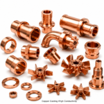
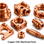
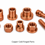
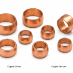
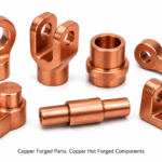
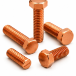
Related Products – Copper Parts and Components
- Copper Hex Bolts, Copper Bolts
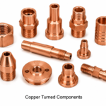
- Copper Turned Components
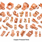
- Copper Pressed Components and Copper Pressed Parts
- Copper Ferrules – Copper Olives
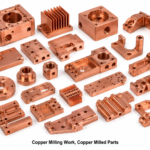
- Copper CNC Machined Parts
- Copper Cold Forged Parts
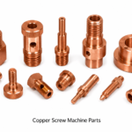
- Copper Screw Machine Parts
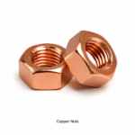
- Copper Nuts
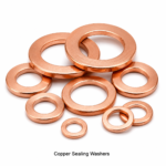
- Copper Sealing Washers
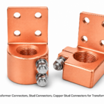
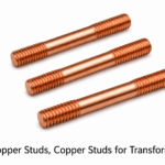
- Copper Transformer Stud Connectors
Request a Quote – Copper Stampings
Electrical Accessories India | Manufacturer & Exporter of Copper Stampings and Pressed Parts
Email: info@elecaccs.com | Website: elecaccs.com
Price: US$ 16.80 / Kilogram (FOB India)
Lead Time: 2–4 weeks | MOQ: 50 Kg | Custom tooling accepted
Submit your drawing or specification (PDF, DXF, STEP) to receive a detailed technical and commercial quotation within 24 business hours. We serve electrical OEMs, EPC contractors, and distributors across India, USA, UK, Germany, UAE, Australia, Canada, Singapore, and South Africa.